Philippe Morey-Chaisemartin, Eric Beisser
Xyalis, France
Conference: SPIE Photomask 2011, Monterey, CA, USA
ABSTRACT
Some chip manufacturing steps lead to non-negligible process variation at wafer level. Typically, chemo-mechanical planarization, known as CMP, is a non-homogeneous process and thickness variations can be measured depending on the distance from a specific die to the wafer center.
These variations have an impact on chip performances and thus on the final yield. This effect may be amplified by the fact that thickness variations on processed wafers introduce focus issues during later photo-lithography steps.
Original chip layouts are modified by inserting dummies to correct thickness variation issues due to CMP, but these correction are based on models only depending on average values.
In this paper, we propose a methodology to replace a single instance of the field written on the mask by multiple instances of this field as commonly used for Multi Layer Reticles. In the described methodology, each field of a same mask does not consist in different layers of the same chip, but of an optimized image of the same layer of the chip.
1 Introduction
In all classical CMP yield enhancement methods, layout optimization is made by inserting dummy shapes in the original design according to average process parameters based on intra-die variations.4,10 In addition to intra-die variations7many studies have highlighted wafer scale variations.2 These process variations may have a big impact on chip performances and may lead either to non functional chips or to out of specs performances.
This is more and more critical with the evolution of technology nodes.1,3Hopefully, CMP process variations across wafer are almost predictable. In this paper, we will describe how to improve the global yield by adjusting the classical layout optimizations.
The DFM optimizations will be performed on the chip by taking into account, not only the average parameters of the process, but also an additional parameter, which is the distance from the die to the wafer center. This optimization can be applied either for the dummy insertion procedure or for optical proximity corrections.
In the first case, the goal is to lower thickness variations across the wafer. In the second case, the goal is to take into account existing thickness variations in the OPC model.5 In both cases, variants of the original layout will be built and placed on the same mask as different fields.
In this paper, we will analyze the thickness variations measured on wafers with standard processes and their impact on the yield. We will propose a die placement driven methodology to adjust the models used for both dummy insertion and OPC. A detailed analysis of the final cost will be presented. Finally, a procedure to automatically generate the step plan to shoot each optimized field on the wafer will be described.
Thanks to the combination of classical mask techniques: MLR, model based CMP and model based OPC, we propose an original methodology to improve wafer processing yield that do not need any specific equipment and at a restricted extra cost.
2 Methodology
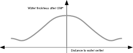
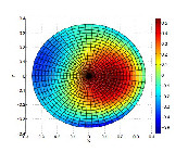
As clearly described in,8 process variations can be spread into intra-die variations and inter-die variations. For CMP process, these wafer scale variations can be easily measured. A statistical analysis of the thickness variation due to CMP is described in next figure.

Figure 1: Typical thickness variation
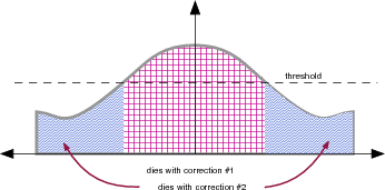
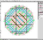
In classical flows, the dummy patterns generation performed to minimize thickness variations after CMP is made at die level and based on average values across the wafer. The dummies insertion procedures are most of the time model based. The models take into account some design specific parameters such as the pattern density as well as physical parameters such as slurry characteristics. We propose to add a new parameter based on the distance from the chip to wafer center. Of course, we can’t generate a specific filling for each die, but we can define different regions based on an estimated thickness variation threshold. Each die belonging to a given region of the wafer will be processed with adapted parameters. With only one threshold value, we define 2 regions on the wafer as shown in next figure.

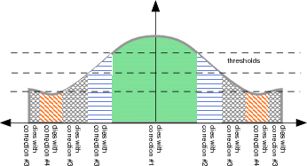
If we use 3 different threshold values me may define 5 different regions as described in next figure.

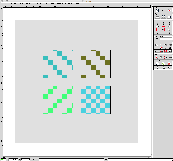
The more threshold values are defined, the more accurate the CMP model will be. But this may lead to a dramatic increase of mask cost as well as a complex photolithography procedure. A classical technique for reducing the mask cost is to use one single reticle for different layers. In this case, the reticle may be spilt into 2 or 4 fields.
Each field being the image of one layer. The method is known as MLR: Multi Layer Reticles. We propose to use this technique, to instantiate on a single reticle, not different layers, but the different versions of a single layer. Each field will be the result of the optimization of the dummies insertion procedure according to the different regions on the wafer.
By using such a technique, we can keep a constant cost for the full mask set. The extra cost will only be related to the increased exposure time during photolithography as each shot will cover either 1/2 or 1/4 of the maximum field. This method can also be used to fix de-focus issues due to wafer thickness variations.5 In this case the OPC model may take into account this thickness parameter and the full OPC is applied to the layer according to the different identified region across the wafer. It may also be possible to adjust the OPC “dynamically”.
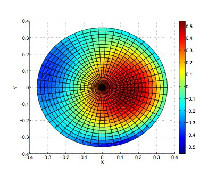
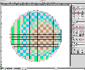
This means that the photo shot of one specific field in a region of the wafer may be adjusted specifically for one wafer. If, for example, the thickness variation is not symmetrical as expected, but is distributed as shown in next figure as described in8 the attachment of each field to the different regions of the wafer may be adapted.

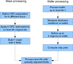
This of course, requires to make measurement on each wafer and will lead to a much more complex process, but when each parameter should be adjusted perfectly to reach an acceptable yield, this technique may bring a solution.Figure 5: process flowchart with dynamic OPC optimization
Figure 5: process flowchart with dynamic OPC optimization
3 Cost optimization
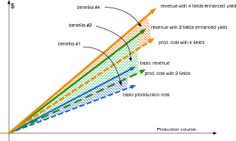
The global cost depends on one hand on the extra cost of chip manufacturing and on the other hand on the benefits brought by yield improvement. The extra cost of chip manufacturing is due to the smaller fields used as done for Multi Layer Reticles. This detailed cost analysis reveals whether, depending on expected variations, a two-field or a four-field reticle should be chosen.

The choice between no multiple fields, 2 fields or 4 fields may be done independently for each layer. The choice criteria will mostly depend on the expected process variations at wafer level and on their impact regarding chip performances. A de-focus variation at gate level may have a dramatic impact on the global yield. As clearly described in,11 photo-lithography is the most important point in the wafer production cost. Revenues are directly related to global yield which itself depends on the photo-lithography performances. Based on the yield estimation described in the above mentionned paper, we can expect a non negligible impact on global yield when applying the described methodology. Using accurate models to fix the systematic wafer level variations will definitively enhance CD accuracy. 4.
4 Step plan
As decribed above, the different fields of the reticle should be attached to the different regions of the wafer according to the optimization criterias. The wafer map is an homogeneous array of dies.


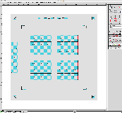
Figure 7: MLR floor plan and wafer map Using different fields on the same reticle to shoot different images on the wafer is commonly used to print some process control modules across the wafer. Driving the stepper (or scanner) to shoot either the field corresponding to basic die or the field corresponding to the PCM is made through a step plan. In our case, the step plan, i.e. the description on the placement of each photo shot on the wafer, can be automatically generated according to the differenet threshold defined.
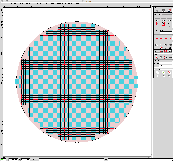
Figure 8: Step plans related to different fields As mentionned above, the step plans can be computed once for all with an estimated process variation across the wafer, or adjusted against the real variations measured during the process. Next figure represents a step plan adjusted during wafer process to exacly match wafer thickness variations.
Figure 9: Dynamically adjusted step plan In both cases, the photo lithography step will be lenghtened due to the fact that each photo shot will cover only a reduced amount of chip compared to a full field photo shot, but hopefully the different instances of the die are all on the same reticle and the whole process is done with one single mask. 5.
5 Conclusion
We have described a method to improve yield by applying much more accurate models. This method allows to take into account wafer level process variations, which was impossible with classical approaches. The described technique can be used either for dummy insertion procedures to improve CMP process yield, or to OPC procedures to take into account de-focus parameters introduced by CMP. By using a classical technique (MLR), we can keep a constant mask cost, which is a critical point in global production cost for advanced technology nodes. It is important to notice that these enhancements don’t use any specific equipment and do not require new procedures.
REFERENCES
1. Frank Fox Anantha P. Chandrakasan, William J. Bowhill. Design of High-Performance Microprocessor Circuits, chapter Models of process variations in device and interconnect, pages 98–115. Number 6. Wiley-IEEE Press, 2000. 2. Lerong Cheng, Puneet Gupta, Costas Spanos, Kun Qian, and Lei He. Physically justifiable die-level modeling of spatial variation in view of systematic across wafer variability. In Proceedings of the 46th Annual Design Automation Conference, DAC ’09, pages 104–109, New York, NY, USA, 2009. ACM.
3. G. Gielen, P. De Wit, E. Maricau, J. Loeckx, J. Martín-Martínez, B. Kaczer, G. Groeseneken, R. Rodríguez, and M. Nafría. Emerging yield and reliability challenges in nanometer cmos technologies. In Proceedings of the conference on Design, automation and test in Europe, DATE ’08, pages 1322–1327, New York, NY, USA, 2008. ACM.
4. Puneet Gupta and Andrew B. Kahng. Manufacturing-aware physical design. In Proceedings of the 2003 IEEE/ACM international conference on Computer-aided design, ICCAD ’03, pages 681–, Washington, DC, USA, 2003. IEEE Computer Society.
5. Andrew B. Kahng, Swamy Muddu, and Puneet Sharma. Defocus-aware leakage estimation and control. In Proceedings of the 2005 international symposium on Low power electronics and design, ISLPED ’05, pages 263–268, New York, NY, USA, 2005. ACM.
6. Dornfeld David A Luo Jianfeng. Wafer-scale cmp modeling of with-in wafer non-uniformity. LMA Reports, University of California at Berkeley, pages 136–157, 2002-2003.
7. Vikas Mehrotra, Shiou Lin Sam, Duane Boning, Anantha Chandrakasan, Rakesh Vallishayee, and Sani Nassif. A methodology for modeling the effects of systematic within-die interconnect and device variation on circuit performance. In Proceedings of the 37th Annual Design Automation Conference, DAC ’00, pages 172–175, New York, NY, USA, 2000. ACM.
8. Kedar Kantilal Patel. Intrinsic and systematic variability in nanometer CMOS technologies. PhD thesis, University of California, Berkeley, 2011.
9. E. Chang D. Ouma-D. Boning J. Chung R. Divecha, B. Stine. Assessing and characterizing inter- and intra-die variation using a statistical metrology framework: A cmp case study. Journal of The Electrochemical Society, 147(11), 2000.
10. Subarna Sinha, Jianfeng Luo, and Charles Chiang. Model based layout pattern dependent metal filling algorithm for improved chip surface uniformity in the copper process. In Proceedings of the 2007 Asia and South Pacific Design Automation Conference, ASP-DAC ’07, pages 1–6, Washington, DC, USA, 2007. IEEE Computer Society. 11. A. H.-I. Lee M. Y. Liao W. L. Pearn, H. Y. Kang. Photolithography control in wafer fabrication based on process capability indices with multiple characteristics. EEE TRANSACTIONS ON SEMICONDUCTOR MANUFACTURING, 22(3), August 2009.
12. Qiaolin Zhang. Across-wafer cd uniformity control through lithography and etch process: Experimental verification. SPIE Advanced Lithography, Vol. 6518(77), 2007.
