

Beyond Tapeout: Opening the Dark Side of Mask Data Preparation
Resources, white papers, articles
Beyond Tapeout: Opening the Dark Side of Mask Data Preparation
How XYALIS Bridges the Critical Automation Gap from Design to Manufacturing
Abstract
The transition from design completion (tapeout) to chip fabrication is often presented as seamless, almost magical. However, this perception overlooks a critical reality: a physical mask set must first be manufactured to transfer the layout image onto silicon. Mask data preparation (MDP) remains something of a black art, presenting intricate technical and economic challenges that demand advanced expertise. While the industry has invested heavily in automating computationally intensive processes like Optical Proximity Correction (OPC) and fracturing, mask layout generation remains significantly under-automated, creating bottlenecks and scalability limitations. This paper examines the critical challenges in mask data preparation and demonstrates how XYALIS solutions address these automation gaps to streamline the path from chip design to manufacturing.
Introduction: Unveiling the Hidden Complexity of Post-Tapeout Processing
When semiconductor chip development flows are presented, the step between chip layout and manufactured chip is often summarized by a magical arrow. This tends to trivialize the transition from the GDS or OASIS® layout to the fabricated chip, which involves numerous sophisticated steps, with mask data preparation representing one of the most technically demanding yet underappreciated phases.
Despite significant industry investments in automating critical processes like Optical Proximity Correction and fracturing, mask layout generation remains an underserved area. Many organizations continue to rely on manual or semi-automated processes for mask layout—workflows that often date back decades—creating inefficiencies, introducing error-prone operations, and limiting scalability with increasing design complexity.
At XYALIS, mask layout is central to our expertise and innovation. We recognize that masks serve as the vital link between chip design and physical manufacturing. The data contained within these masks directly inform the mask and silicon production process, making thorough mask data preparation essential for achieving successful manufacturing results.
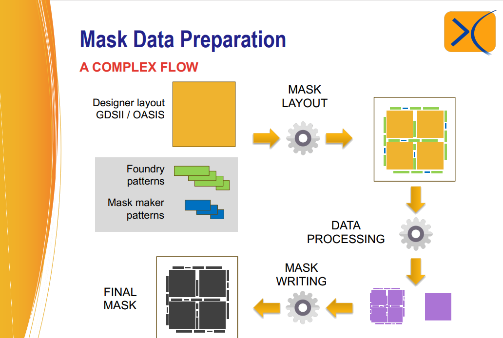
The Complete Mask Data Preparation Pipeline
From Design Data to Manufacturing-Ready Masks
Photomasks, produced through advanced techniques involving light-sensitive materials and precisely engineered patterns, play a critical role in transferring integrated circuit designs onto silicon wafers. Modern mask preparation demands an integrated process that handles everything from 4x or 5x pattern scaling to the inclusion of metrology, alignment, mask shop structures, and foundry-specific patterns, all while ensuring seamless integration with complex chip layouts.
This transformation—beginning from design data (GDS or OASIS® files) and ending with manufacturing-ready masks—involves a carefully orchestrated, multi-stage pipeline that balances efficiency, accuracy, and manufacturability:
- Chip-Level Dummy Fill: Initial density optimization within each chip design before flattening operations to ensure homogeneous density distribution – could be done before or after tapeout
- Database Flattening: Flattening the hierarchical structure of layout files to enable efficient downstream processing.
- Merge Operations: Merging individual chip databases to prepare for reticle-level processing – can be done later in the flow as well
- Build Field: Before any reticle can be used for photolithography, individual chip layouts must first be systematically arranged in an array within the reticle exposure field. This careful placement ensures efficient use of silicon, creation of scribe lines between chips and enables wafer sawing. In standard production, identical chips populate the field, but in certain cases—such as Multiple Project Wafer (MPW) aka shuttle runs—different chip designs may be floor-planned together within the same field. MPW, an optional strategy, enables cost-effective prototyping, test chips or low-volume production by sharing mask and wafer space among various projects, further complicating the arrangement but maximizing resource utilization.
- Frame Generation: During this phase, the focus is on establishing the frame layout and its contents such as test structures to support metrology, lithography, process control monitoring (PCM), and other essential functions. It must meet complex process specific placement constraints coming from the different teams who have generated these test structures. Respecting the specifications of frame features and their placement constraints ensures that all downstream processes—inspection, alignment, and quality assurance—are seamlessly supported by the information embedded in the frame.
- Reticle-Level Dummy Fill: Applying further density optimization at the reticle level after chip and frame structures placement for uniformity.
- Sizing: Making geometric adjustments to layout features to account for process variations and manufacturing tolerances.
- OPC Application: Applying Optical Proximity Correction to layout shapes, which significantly increases data complexity and file size.
- Fracturing: Decomposing complex shapes into simple geometric primitives that can be processed by mask writing equipment.
- Mask layout: in this stage additional features vital for efficient mask manufacturing, ongoing mask management, optimal mask utilization, and precise alignment are added to the field or fields. This step involves methodically inserting reference marks and alignment features, all while adhering to foundry and mask shop specifications.
- Step Plan and Wafer Map Optimization: Generating exposure sequences and wafer-level optimization strategies to maximize throughput and yield.
Critical Challenges: The High-Stakes Environment of Mask Manufacturing
Economic Imperatives Drive Automation Needs
The economic stakes of mask manufacturing are staggering. A single 32nm mask set costs approximately $1 million to produce, and any error cascades across every wafer in production. This demands a “zero-defect” environment, where automation becomes not just an efficiency consideration, but an essential business safeguard. Despite automation advances in OPC and fracturing, frame and mask layout generation remain under-automated in many organizations, creating inefficiencies, escalating error risks, and imposing scalability limitations that impact manufacturing timelines and costs.
Data Volume Explosion
Modern semiconductor manufacturing faces unprecedented data challenges. Individual devices involve dozens of layers, each containing billions of polygons, with complete mask sets reaching multi-terabyte sizes and individual layers as large as 10-100GB. OPC processing further amplifies these challenges, increasing database sizes by up to 10x as simple geometric shapes transform into complex polygons with numerous Sub-Resolution Assist Features (SRAFs). Managing these vast data volumes requires high-performance computing infrastructure and specialized tools.
Multi-Criteria Optimization Complexity
Frame and mask layout generation represents a sophisticated optimization challenge involving multiple competing requirements:
- Critical Pattern Integration: Modern photomasks must accommodate foundry and mask shop patterns requirements:
- Lithography, test, metrology and PCM Patterns: These specialized patterns enable precise measurement and control of manufacturing deformations, ensuring consistent quality across the entire wafer.
- Alignment Patterns: Achieving nanometer-scale precision requires sophisticated alignment patterns that enable accurate layer-to-layer registration during the multi-step manufacturing process.
- Foundry and Mask Shop Patterns: Additional patterns specific to foundry requirements and mask shop specifications are integrated alongside the core chip layout.
- Identification Patterns: Barcode and title generation for mask tracking and process control.
- Scaling Optimization: Photomasks typically employ 4x or 5x scaling factors to reduce writing time while maintaining precision, representing a careful balance between manufacturing efficiency and accuracy requirements.
- Constraint Management: The integration process must satisfy competing demands from metrology teams, process engineers, and lithography specialists, often involving hundreds of patterns with conflicting placement constraints.
- Density and Layout Optimization: Achieving homogeneous density across layers requires strategic dummy fill placement at both chip and reticle levels, while MPW assembly demands careful planning to optimize silicon utilization and manufacturing efficiency.
These multi-faceted requirements create complex optimization problems that benefit significantly from automation but are frequently handled through manual processes or limited tooling, resulting in suboptimal outcomes and scalability constraints.
Quality Assurance: Meeting Zero-Defect Requirements
1. Validation Imperatives: Given the million-dollar cost of mask sets and the error multiplication effect across wafers, extensive process validation becomes mandatory rather than optional. Every step in the mask data preparation flow must be validated to ensure final masks will produce intended manufacturing results.
2. Validation Complexity and Risk Management: The validation process presents significant challenges: verifying pattern placement accuracy, confirming density optimization effectiveness, and ensuring compliance with foundry and mask shop specifications.
3. Integrated Quality Control: Modern mask data preparation must embed quality control measures throughout the process rather than treating quality as a final checkpoint. This includes automated constraint checking during frame generation, continuous density checking, and integrated pattern placement validation.
Organizations lacking advanced automation tools often manage mask layout generation through manual processes or legacy systems, leading to increased cycle times, elevated error potential, reduced scalability, suboptimal mask utilization, and inconsistent pattern placement—all unacceptable in today’s demanding manufacturing environment.
The XYALIS Solution: Comprehensive Automation for Complex Challenges
XYALIS addresses the complex challenges of mask data preparation through a unified automation platform that directly tackles the high-stakes environment, data volume explosion, and multi-criteria optimization complexity identified above. Our end-to-end solution typically reduces engineering time by 40-70%, and in extreme cases, mask layout generation went from weeks down to an hour, while improving quality and improving silicon usage by 10-15%.
Addressing the Zero-Defect Imperative
The million-dollar cost of mask sets and their error multiplication across wafers demands a fundamentally different approach to quality assurance. XYALIS embeds automated quality verification throughout the entire workflow, eliminating the error multiplication risks inherent to traditional manual processes. Our platform generates correct-by-construction field and mask assemblies that automatically meet customer specifications while continuously validating input layouts through integrated integrity checkers.
This approach transforms process validation from a final checkpoint into an embedded workflow characteristic. Our end-to-end automation of frame integration, fill insertion, mask layout generation, and step plan creation provides the reliability that zero-defect requirements demand.
Managing Data Volume Explosion
The unprecedented scale of modern semiconductor data—with individual layers reaching 10-100GB and complete mask sets creating multi-terabyte datasets—requires specialized processing capabilities that traditional tools cannot provide. As an active member and sometimes leader in advancing OASIS® industry standards(SEMI P39 OASIS® revision task force, SEMI P49 OASIS® curvilinear, SEMI P45 MALY, SEMI P44 OASIS.MASK, and SEMI P10 the mask order form), XYALIS has the expertise in GDS and OASIS® formats to address this challenge, through optimized algorithms and parallelized computation that efficiently manage the massive datasets generated by modern OPC and fracturing operations. Our specialized data representation engine handles the largest designs with maximum performance and minimum memory requirements, enabling organizations to maintain productivity even as data volumes continue their exponential growth.
This high-performance processing capability seamlessly integrates with comprehensive format support across all standard layout and job deck formats, including GDSII, OASIS®, OASIS.MASK, MALY, and MEBES. This compatibility ensures that organizations can leverage advanced processing capabilities without disrupting existing workflows or requiring costly infrastructure changes. The result is a solution that scales with advancing technology nodes rather than becoming a limiting factor.
Solving Multi-Criteria Optimization Complexity
The integration of hundreds or even thousands of patterns with competing constraints from different stakeholders represents one of the most complex optimization challenges in mask data preparation. XYALIS addresses this through a SPECS file using a formal language to define the items to be placed with their constraints, that drives advanced algorithms to automatically handle the intricate integration of lithography, metrology test and PCM patterns, alignment patterns, foundry and mask shop patterns, identification patterns, and scaling optimization requirements. This automated approach eliminates the manual coordination typically required for complex pattern placement decisions while ensuring optimal outcomes across all stakeholder requirements.
Our platform extends this optimization capability to shuttle management, streamlining the integration of multiple chip designs into MPWs through automated conflict resolution and intelligent floorplan optimization.
Field-wide dummy fill and scribe line minimization work together to maximize silicon utilization while maintaining manufacturing requirements across chip, frame, and reticle levels.
The system automatically balances competing demands from metrology teams, process engineers, and lithography specialists, transforming what was once a time-consuming manual negotiation process into an automated optimization routine.
Comprehensive Process Integration and Manufacturing Readiness
Beyond addressing individual challenges, XYALIS provides complete workflow integration that eliminates the manual bottlenecks creating scalability limitations in traditional approaches. Our platform automates the entire process from specifications to manufacturing-ready masks, using user-defined templates to ensure consistency between masks while supporting the newest technologies including 3D-IC masks, stitching, multi-layer reticles, and advanced packaging requirements.
The system automatically generates comprehensive documentation and SEMI-P10 mask order forms, ensuring seamless hand-off to mask shops and manufacturing teams. Step plans and wafer maps are calculated and optimized automatically for either maximum usable chip output or minimum manufacturing time, depending on production priorities. This level of automation extends to customization capabilities through Python API and SQL database connectivity, enabling direct integration into existing customer flows with minimal disruption.
Proven Business Impact and Scalability
Organizations implementing XYALIS solutions consistently achieve 40-70% reduction in engineering time and 10-15% improvement in silicon usage, transforming post-tapeout cycles from days or even weeks to hours while maintaining zero-defect quality requirements. As one customer noted, “XYALIS customizable solution addressed bottlenecks and inefficiencies in our existing MDP flow with their specialized engines and domain expertise.”
These results demonstrate how addressing each critical challenge—from economic risk mitigation to data volume management to multi-criteria optimization—creates compounding benefits that transform the post-tapeout phase from a high-risk bottleneck into a source of competitive advantage. Organizations gain not only immediate efficiency improvements but also the scalability to handle increasing design complexity without proportional increases in engineering resources, enabling faster time-to-market and improved manufacturing outcomes in an increasingly complex semiconductor landscape.
Future Directions: Preparing for Next-Generation Challenges
Emerging Technology Demands
As semiconductor technology advances, mask data preparation faces escalating challenges. Continued feature size reduction and chip complexity growth will further increase data processing requirements, pushing current computational capabilities to their limits. Next-generation lithography techniques, including mask stitching and advanced patterning methods, will require new optimization approaches. Additionally, emerging 3D chip architectures present novel challenges for mask layout and process control, demanding fundamentally different approaches from traditional planar design methodologies.
Strategic Technology Investment
The industry must prepare for these evolving challenges by investing in advanced automation capabilities and next-generation processing technologies capable of handling increased complexity and data volumes of future semiconductor devices. Organizations that proactively adopt comprehensive automation solutions will be best positioned to capitalize on emerging opportunities while maintaining competitive advantages.
Conclusion: Transforming the Dark Side into Competitive Advantage
The post-tapeout journey represents a critical phase in semiconductor development demanding sophisticated tools, processes, and expertise. While the industry has successfully automated OPC and fracturing processes, significant opportunities remain in mask layout generation automation.
XYALIS bridges these automation gaps through comprehensive solutions that streamline workflows through automated processes that eliminate manual bottlenecks, improve quality via automated frame and mask generation ensuring consistency and enforcing placement requirements, enable scalability allowing organizations to handle increasing complexity without proportional resource increases, and optimize costs through efficient automation that reduces engineering expenses and accelerates time-to-market.
The semiconductor industry’s future success depends on recognizing that the tapeout-to-manufacturing journey requires dedicated expertise and innovative automation solutions. By embracing advanced mask data preparation tools like those provided by XYALIS, organizations can transform this critical manufacturing phase from a constraint into a competitive advantage.
The “dark side” beyond tapeout need not remain a bottleneck. With comprehensive automation tools and optimized processes, the path from design to manufacturing becomes a source of competitive differentiation rather than operational limitation.
By Frederic Brault, CTO, XYALIS
-
Categories
- Glossary
- Publications
- Resources
- Whitepapers