CMP Monitoring and Prediction Based Metal Fill
Resources, white papers, articles
CMP Monitoring and Prediction Based Metal Fill
Philippe Morey-Chaisemartin (a), Eric Beisser (a),
Jean-Claude Marin (b), Lidwine Chaize (b), Pascal Guyader (b), Julien Rosa (b)
a: Xyalis – Grenoble – France
b: STmicroelectronics – Crolles – France
Conference: ISQED 2011 – Santa Clara, CA, USA
ABSTRACT
Nowadays, two different methodologies are used to address the CMP issues. On one hand, we find basic design oriented methods consisting of reaching a minimal density of geometries in the design. On the other hand we find model based approaches in which complex process related parameters are used. This makes these techniques, either not accurate or not usable by designers. In both cases there is no efficient monitoring of the CMP effect through Process Control Modules. This paper presents a new methodology to improve CMP process yield from the designer side. A prediction function of metal thickness variations due to CMP is established thanks to specific test structures. A method to monitor the CMP process evolution at no cost is presented and finally a technique for using the prediction function to drive metal filling procedure is described.
1 Introduction
A. Key parameters of Chemical Mechanical Polishing
Many parameters have a critical impact on the CMP process. First of all, we have to distinguish the two different CMP processes: oxide CMP for dielectric planarization and copper CMP for metal removal. Even if techniques are roughly similar, the materials are dramatically different and thus, the related parameters are obviously not the same. In this paper, we will focus on copper CMP which is the most complex. The presented methodology may also apply to oxide CMP (or ILD CMP). We also need to split the parameters impacting CMP into two major categories: the process related parameters (pad pressure, slurry quality, processing time…) on one hand, and the design parameters (layer density, topology…) on the other hand. The process parameters may be adjusted during wafer fabrication depending on technology or equipments variations. We should differentiate process variation from process evolution. We define a process variation as a short term (or local) modification of the results, i.e. variations between two different lots or even wafers of the same lot. A process evolution is a long term slight modification of technology parameters. CMP process has a direct impact on metal thickness. The reduction of copper line thickness is due to erosion or dishing effect. Variation on metal thickness implies a modification of metal line resistance and thus of interconnect delays. It has been measured that a variation of up to 20% in delays due to interconnections may occur. If we roughly consider that interconnect delays are at least half of the global delays, CMP process may lead to a variation of 10% in design performances (best case) or to a non functional chip in case of race conditions[9][7].
Design related parameters need to be taken into account weeks or months before wafer processing and must not depend on any technology variation. The designer may only take into account some process evolutions. We propose a methodology to monitor these evolutions and a way to use this information during design back-end phase in order to improve the yield.
B. The prediction based methodology
Most of the CMP models use process parameters[8]. They help to adjust equipments characteristics during wafer processing. But can’t be used by the designer in order to optimize final layout to improve yield. So, most of the time, a simple rule, based on metal density in each window, is applied. Metal fills are added in order to reach an average density value within these windows[11]. Unfortunately, CMP process is a little bit more complex, and we propose to define a prediction function, less accurate than a real model, but accurate enough at design stage and capable of influencing more precisely metal filling. The idea is to study various layout configurations, to measure the physical variations related to CMP process on these different configurations, then to compare the chip layout to the known standard configuration and predict the expected variations. If needed, a dedicated metal filling engine will then be able to insert the expected dummy geometries in order to modify the layout configuration to be as close as possible to a “good” topology, i.e. a configuration that creates variations within allowed range.
II. DESIGN INFLUENCE
A. Adjustable parameters
There are quite a few parameters on which the designer may interact. Density is the most common and in all classical approaches, it’s the only parameter taken into account to drive metal filling. We have identified two other parameters: roughness and topology. • Roughness is a measurement of the number of transitions between copper and dielectric. It can be measured by the sum of perimeter of all polygons. • Topology is a little bit more difficult to formalize: its directly related to the shape of the polygons.
We can roughly differentiate regular stripes from random polygons. We will focus on these 3 parameters, with a priority on density and roughness as these are the factors that can be more easily adjusted during layout or place and route phase of the design. The measure of the density is a simple value between 0 and 1, but the roughness is more complex as it is related to the sum of the perimeters of the polygons in a given area. This value is directly related to process node and has no default maximum value. In order to normalize this value, we will take into account the minimum pitch of copper and consider that the maximum roughness is obtained with the smallest possible squares of metal placed with the minimum spacing. We will then be able to define the roughness also as a value between 0 and 1. A value of “1” corresponds to the highest possible roughness for the current process and layer. Other parameters like gradient [3]may also be used during metal filling step but are not relevant during initial analysis.
B. Validation methodology
The methodology consists in measuring the impact of the 3 design parameters on the CMP process and thus on the metal thickness variation. We will correlate the physical thickness variation to an electrical variation easily measurable. A set of test structures should be available in order to make a statistical analysis on the various results. This means that, for each parameter, we should implement a set of different patterns with one of the parameters changing, the 2 other remaining fixed. This may create a number of different patterns, but considering that some configurations are not possible and that some combinations may be redundant we can dramatically decrease the number of test structures. The validation of the process monitoring structure is made in multiple steps:
• implement as much as possible different structures on a test wafer
• electrically measure the structures
• physically measure the metal thickness
• establish the correlation
• define a prediction function ? = f (D,R, T) with
– ? = copper thickness,
– D = density,
– R = roughness,
– T = topology.
Once the process monitoring structures are validated, we will be able to:
• Estimate impact of CMP by applying the prediction model to all newly designed chip in production
• Slightly modify the layout by inserting dummy filling patterns in order to be as close as possible to a “good” configuration.
An accurate monitoring of process evolution will be performed in order to:
• Improve and adjust the prediction model by inserting parametrized test structures in all new MPW projects.
See IV-A.
III. THICKNESS VARIATION MEASUREMENT
A. Expected variations
The prediction models must be as accurate as possible, but the measure errors are not negligible. To get accurate results, we must either perform enough measurements to statistically remove all the “noise” of the measure by itself, or build test structures that are able to provide the expected value (without error) by correlating 2 different measures. As the test is always time consuming, and because yield improvement is not only a matter of loss of silicon but also a matter of lost of time, the second solution has been chosen even if more complex. Thickness variation of metal wires leads to a resistance variation of this wire. Resistance variation is easy to measure, but for advanced technologies (65nm and below) many other parameters may introduce a variation on metal resistor. It is then very important to clearly identify what is due to CMP from what is due to any other process variation. The full analysis is made through 2 complementary measures: resistance of a long metal wire and capacitor between this wire and an overlapping wire in above metal layer (Fig 1). The two wires will be folded as serpentine in order to fit in a restricted area. A thickness variation on copper layer will result in: • a variation of the resistor of the serpentine • a variation of the capacitor made of the 2 overlapping serpentine layers
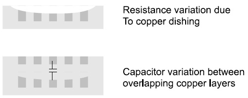
Figure 1. Copper dishing impact on electrical parameters As the measure structure must be as small as possible, the capacitor made from the two overlapping serpentines will remain very low and very difficult to measure accurately. So, we will not directly measure this capacitor but the cut-off frequency of a low pass filter made of the resistance and capacitance of the metal wire (Fig 2).
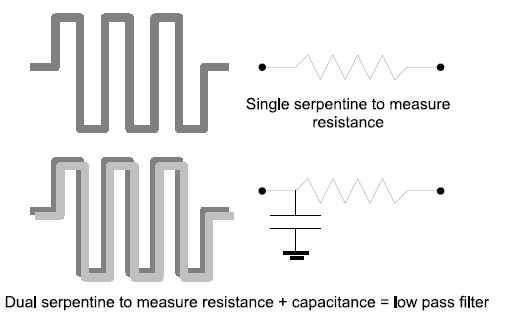
Figure 2.
Dual measure The cut frequency of the low pass filter can is defined by: 
• With: – ?: resistivity, – ?: permittivity, – e: inter-layer space, – h: copper thickness, – L: copper path length. Unfortunately, the reduction of metal wire thickness leads on the increase of the resistance and on the reduction of the capacitor in the same time. But if we carefully study the cut frequency function depending on the thickness variation of metal wires, we obtain the curves of figure 3. 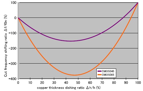
Figure 3. Dependence between copper thickness and cutoff frequency Cut frequency function is not a linear function and 2 different values of thickness variation may be deduced from frequency measure. But we can easily compute capacitor from cut frequency f0. We then compare with cut frequency f0,1 of a higher density test structure where we expect to have a greater dishing ratio. We will then be able to deduce the exact thickness variation ?h: • if f0,1 is lower, ?h being higher, then slope is negative. • if f0,1 is higher, ?h being higher, then slope is positive. See figure 4. 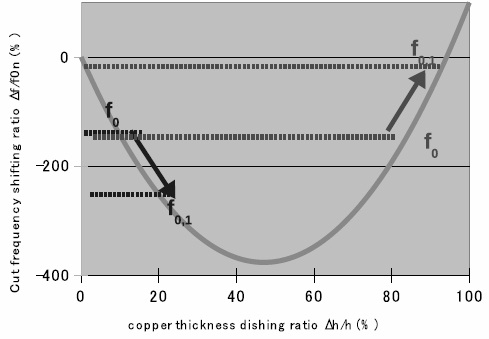
Figure 4. Measure correlation
B. Test structures
1) Constraints: The CMP monitoring structures should be large enough to measure CMP impact within a wide area (up to a few hundreds of microns). The goal is to provide test structures that can be adjusted to fit in any available area on silicon. We need to develop CMP monitoring structure: • flexible to fit in any empty areas of a Multi Project Wafer (MPW), i.e. an assembly of heterogeneous dies usually used for prototypes or test purposes. • offering an access to the multiple available parameters • easily measurable (electrically) Each test structure will be made of two different parts (fig 5): • the environment that should offer the expected characteristics of the multiple criteria: density, roughness and topology • the measured structure that will be surrounded by the “environment” and that should allow to accurately measure the metal thickness variation (copper dishing ratio). 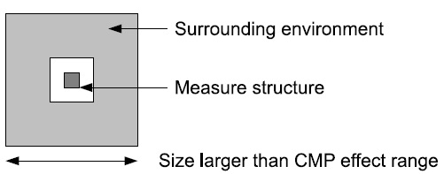
Figure 5. CMP monitoring structure 2) The CMP sensitive environment: Each surrounding environment structure must provide one defined configuration, i.e. density, roughness and topology. An automatic generator has been developed to draw all requested polygons to meet the requirements. The generator is able to create a set of test surrounding environments by fixing 2 parameters and changing the third one (by steps) in all the possible range. The topology parameter has been restricted to 2 possibilities: regular stripes or regular squares. The size of the surrounding environment as well as the center space, left free to place the measurement structure, are user defined. For each topology (lines and squares), a set of different environments has been selected as described in figure 6. 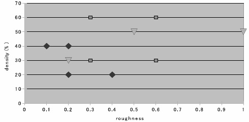
Figure 6. List of pre-defined environments 3) The measured structure: The measured structure will always remain the same (for a given metal layer). It will not depend on the surrounding environment. The pattern should be small enough, not to impact the global environment by its own characteristics, and large enough to show evidences of variations. Too small structures will lead to very small variations in terms of resistors or capacitors and may not be distinguished from measure errors. The thickness variation (i.e. copper dishing ratio) will be measured thanks to the resistor variation of a copper line. This copper line will be folded as a serpentine to fit in the smaller possible area. As mentioned in chapter III-A, the measure must be validated through the correlation with a second measurement. A second serpentine in above copper layer will exactly overlap the resistor serpentine. Layout of the serpentine are automatically generated by a piece of software. Test measurement structure width and height, as well as metal width and pitch are user defined.
C. Measurements
The different test structures have been inserted in a 65nm shuttle. This process has been chosen to validate the methodology because of its maturity. It is then easier to validate the correlation between the various parameters and measurement results. If we also consider the cut frequency function as described in figure 3, we can see that it is easier to get accurate results for dishing ratio variation for 65nm than for 45nm process. This will help to validate the whole methodology and calibrate the prediction function. Once this method is qualified, it will be easy to adapt it to next technology nodes: 45nm, 32nm, 28nm…. 1) Electrical measures: A full set of different test structures has been electrically measured through the whole wafer. Table I presents the average value of the resistor for metal 2
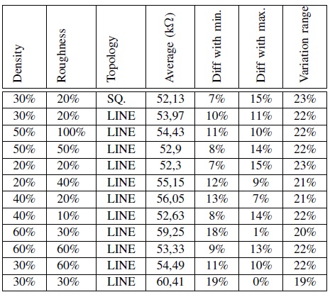
Table I RESISTOR MEASUREMENT ACCORDING TO TOPOLOGY We can see that we have a variation range of about 23% on the metal wire resistance depending on the topology of the surrounding area. All available sites on the wafer have been measured with a variation of less than 5% across the wafer for a given test structure. We can then confirm that this variation is only due to the topology configuration surrounding each test structure. Additional measures made on the cut frequency of the low pass filter made of the copper line resistor and the coupling capacitor between the 2 overlapping metal wires leads to the same results. Partial results are presented in table II. 2) Thickness measures: Thanks to Scanning Electron Microscopy (SEM), measurement of copper lines thickness have been performed on silicon. Partial results are presented in table III We can also verify that the variation range is also within 20%. We also have made a correlation between the results
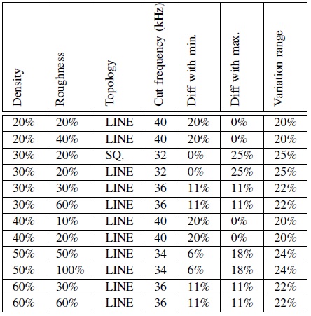
Table II CUT FREQUENCY OF LOW PASS FILTER
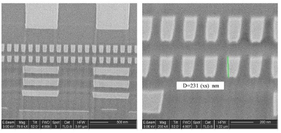
Figure 7. Cross section of test serpentine obtained with SEM obtained through the 3 different methods. The results for thickness and cut-off frequency have been obtained through single measures and may be corrupted by some measurement errors. We have removed the 2 most extreme results, so that the correlation between the different results can be more easily established. These results are shown in figures 8 and 9. 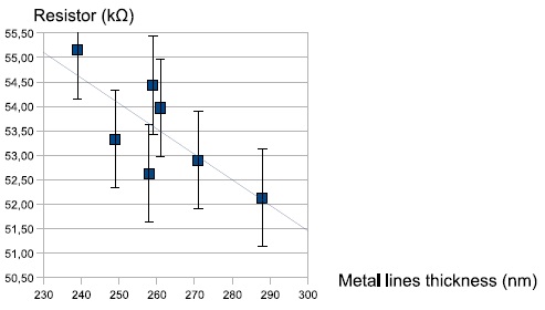
Figure 8. Line resistor vs. metal thickness The results obtained clearly show the relation between thickness and electrical measurements. The cut-of frequency lets appear less dispersion. It confirms that dual measures by different methods are mandatory to get an accurate estimation of the thickness. Additional measures will be performed to validate the correlation function through a statistical approach.
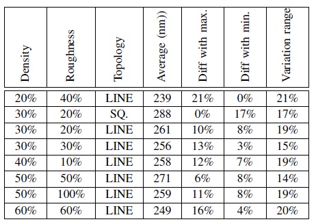
Table III COPPER LINES THICKNESS
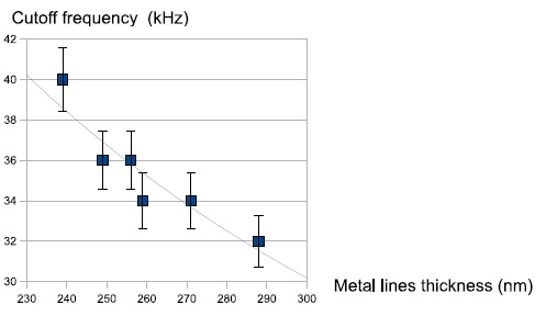
Figure 9. Cut-off frequency vs. metal thickness
IV. PROCESS MONITORING
Obtaining accurate measurements to establish a prediction function is the first step of the methodology. As we focus on advanced technologies, some variation may occur while the process becomes more mature. We need to be able to monitor any variation in order to adjust the prediction function when needed.
A. Using shuttles
Due to the price of mask sets and to the fact that first time silicon success is more and more challenging because of the design complexity, MPW (or shuttles) are now launched by most of the foundries on a regular basis. All these MPW are assemblies of multiple sizes rectangular shapes. Small areas remain empty between the dies. They are too small to place any chip but larger than basic scribe lines and typically large enough to place CMP test structures. 1) Benefits: All the remaining areas between the dies in a MPW must be filled with dummy layers in order to avoid any CMP issue on neighbour dies. The shape of theses areas may change but as soon as we can identify a rectangular area large enough to embed a test structure, we can automatically generate such a structure thanks to the automaticgenerator developed . By using this method, CMP monitoring is made at absolutely no cost in term of silicon area. 2) Automatic generation of PCM: The requested area to place a monitoring structure is about 500? in the worst case. CMP effects with a wider range (1 millimeter or more) may not be measured by such a method and, anyway, cannot be fixed through local design optimization. We only focus on short range CMP effect (between 50 a a few hundreds of microns). So, depending on the process characteristics, this area may be reduced to 200 or 300?. Once identified, each empty area will be filled by one ore more CMP monitoring structures. The choice of the parameters used to generate each structure will depend on the number of structure which can be generated. The probing pads connected to the test structure will be inserted in the standard scribe lines surrounding the originally empty area (Fig 10). An automatic routing between probing pads and the test structure must be done. 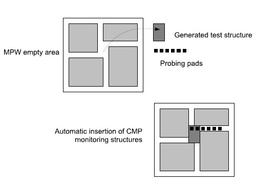
Figure 10. Insertion of monitoring structures in an MPW
B. Yield improvement
1) Statistic analysis: Thanks to the various measures made on first test wafer, and to the refinement obtained through each shuttle, we can elaborate a prediction function. This prediction function may either be obtained by a statistical method as described in [10]and [2] or a simple look-up table. 2) Design feedback: There are many different methods used for metal filling: either based on physical models or based on a simple density target [5][4][6]. In the proposed methodology, a parameter extraction is performed on the layout database. This extraction provides the current values for the different key parameters (density, roughness and topology) on a window basis. On each window, we will automatically compare the set of values with the different test structure configurations already measured on silicon. The prediction function will return an average thickness variation and the designer will be able to validate the current layout. If the variation is out of allowed range, an automatic filling tool will insert dummies in order to reach a set of parameters which leads to an acceptable configuration (Fig 11). A specific tool able to take into account both density and roughness has been developed and has been fully qualified. This tool is also capable of instantiating rectangular dummies as well as stripes or any complex shape in order to also meet topology requirements.
V. CONCLUSIONS
We have developed a generator of CMP monitoring structures to analyze CMP effects according to a various set of predefined configurations. These monitoring modules have 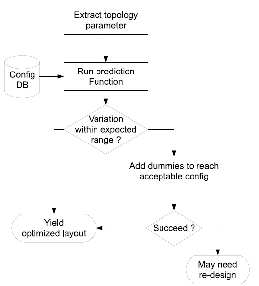
Figure 11. Dummy filling flow been processed on a 65nm multi project wafer. Electrical measurements have been performed and physical measurement of metal thickness have been made with a SEM (Scanning Electron Microscope). Correlation between the various results have allowed to establish a prediction function. This prediction function can be applied on any area of a real chip to drive a metal filling engine which is already available. To validate the full methodology, the different steps (insertion of process monitoring modules, electrical measures, physical measures) have been performed manually but the procedure can easily be automatized to fulfill production requirements. The monitoring structures generator will be refined to automatically take into account process design rules as well as MPW floor plan. The prediction function established with a restricted number of cases may be enhanced at each new shuttle and thanks to a fully automatic test protocol. This project has been sponsored by European program Catrene[1]. It has been developed in collaboration between Xyalis and STmicroelectronics.
REFERENCES
[1] Highly optimised design methods for yield and reliability. WEB, july 2007.
[2] A. Ollivier A. Noire, S. Bergeon and Y. Courant. Design of st planar integrated inductors based on infiniscale flow. In ICICDT, June 2008.
[3] Huang-Yu Chen, Szu-Jui Chou, and Yao-Wen Chang. Density gradient minimization with coupling-constrained dummy fill for cmp control. In ISPD ’10: Proceedings of the 19th international symposium on Physical design, pages 105–111, New York, NY, USA, 2010. ACM.
[4] Yu Chen, Puneet Gupta, and Andrew B. Kahng. Performance-impact limited area fill synthesis. In DAC ’03: Proceedings of the 40th annual Design Automation Conference, pages 22–27, New York, NY, USA, 2003. ACM.
[5] Yu Chen, Andrew B. Kahng, Gabriel Robins, and Alexander Zelikovsky. Closing the smoothness and uniformity gap in area fill synthesis. In ISPD ’02: Proceedings of the 2002 international symposium on Physical design, pages 137–142, New York, NY, USA, 2002. ACM.
[6] Chunyang Feng, Hai Zhou, Changhao Yan, Jun Tao, and Xuan Zeng. Provably good and practically efficient algorithms for cmp dummy fill. In DAC ’09: Proceedings of the 46th Annual Design Automation Conference, pages 539–544, New York, NY, USA, 2009. ACM.
[7] Puneet Gupta and Andrew B. Kahng. Manufacturing-aware physical design. In ICCAD ’03: Proceedings of the 2003 IEEE/ACM international conference on Computer-aided design, page 681, Washington, DC, USA, 2003. IEEE Computer Society.
[8] A. B. Kahng and K. Samadi. Cmp fill synthesis: A survey of recent studies. 27(1):3–19, 2008.
[9] Arthur Nieuwoudt, Jamil Kawa, and Yehia Massoud. Impact of dummy filling techniques on interconnect capacitance and planarization in nanoscale process technology. In GLSVLSI ’08: Proceedings of the 18th ACM Great Lakes symposium on VLSI, pages 151–154, New York, NY, USA, 2008. ACM.
[10] P. FrR´ res J.M. Verilhac R. Coppard I. Chartier Y. Courant V. Fischer F. Mohamed S. Jacob, R. Gwoziecki. Fast and reliable compact model for organic electronic devices using behavioral modeling methods. In LOPE-C, June 2009.
[11] Yaoguang Wei and Sachin S. Sapatnekar. Dummy fill optimization for enhanced manufacturability. In ISPD ’10: Proceedings of the 19th international symposium on Physical design, pages 97–104, New York, NY, USA, 2010. ACM.
-
Categories
- Glossary
- Publications
- Resources
- Whitepapers


