

Using a Mask Rule Checker as an Electrical Rule Checker
Resources, white papers, articles
Using a Mask Rule Checker as an Electrical Rule Checker
Philippe Morey, Eric Beisser
XYALIS – Grenoble – France
Conference: Photomask and NGL Mask Technology, June, 2013, Yokohama, Japan
ABSTRACT
Design complexity sometimes grows faster than EDA tools performances, and some innovation should be made on the design flow to guarantee the best possible validation in a reasonable time. This was the challenge we were facing for the final layout validation of a 3 billions transistors, multi cores chip designed for a 28nm process. The design backend validation requires multiple tools: the LVS to check connectivity, the DRC to check layout rules and the ERC to check any risk of power drop among the whole chip. While the 2 first tools are able to deal with huge designs by using hierarchical approaches, Electrical Rule Checking is much more complicated as the power routing is generally made flat at the top level of the chip.
The classical ERC tools were not able to validate the power distribution at top level. The power distribution was made through a power grid using two metal layers and arrays of vias to connect each block at deeper metal layers. The chip is made of 256 processors and has a quite regular structure so that each module has it own power grid with the same pitch and every thing should be butting or properly connected at top level. It has then been decided to use a very efficient tool dedicated to geometrical verification of flat designs (typically a Mask Rule Checker) to check any interruption on power lines or missing vias in arrays. This paper will describe how this validation was performed as well as the performances obtained on a 28nm, 3 billions transistors design.
ELECTRICAL RULES CHECKING
Basically, all electrical rules are validated through a dedicated software: the Electrical Rule Checker. Many different kind of checks are performed by such tool, from well polarization to voltage drop depending on blocks activity. This requires a huge amount of data and computation time. An ERC generally first build a netlist including all parasitic resistors. Wires and vias cannot be considered anymore as simple connections but are represented as resistors in order to compute voltage drop according to power consumption. This methodology is very efficient when only addressing small chips or single blocks of a chip. For very big designs such as the example on which we were involved, the global netlist including parasitics becomes too large to expect a reasonable computing time and reliable results. Even with advanced computation algorithms,[1],[2] the problem remains complex and the computation time is far from being negligible in a design flow loop. Anyway, an exhaustive Electrical Rule Check should be part of the final validation flow as mentioned in [4]. Some studies have already been carried out to improve this critical step in design verification6and we will present our contribution in this domain.
A SPECIFIC CASE
Regular matrix of processors
Our study case was a massively parallel processor array. It was made of 256 cores, organized in clusters, with embedded memories, interconnected through a high bandwidth Network on Chip [3]. With a structure for which each core, or at least small clusters of cores, are all identical, it is possible to carefully analyze power consumption at processor level with a classical Electrical Rule Checker. Then, the power distribution, made at top level, may be validated separately and possibly with a dedicated strategy. So it has been decided to split the validation in two parts.
- A full and deep analysis of one cluster including a couple of processors, through ERC.
- The analysis of global power distribution at top level.
Power consumption is almost uniform at top level. As the data processing is uniformly distributed on the array, by construction, the power consumption is the same for each processor and is not related to the activity of the different cores as they are all identical. The only mandatory check was then to insure that each processor was correctly connected to power supply through the same minimal resistor network.
Power Grid
The goal of this work was not to achieve a full electrical rule check down to the transistor level or related to the miscellaneous blocks activity, but to check the top level power distribution. The two upper metal layers, which are generally thicker than other ones, are usually dedicated to power distribution. A power grid is built by alternating the different power lines horizontally and vertically. At least two grids are interlaced for VDD and GND, but additional grids may be added in case of multiple power supplies. Horizontal and vertical lines of each grid are interconnected through vias.
Each via being quite resistive, it is expected to have the maximum number of vias at each intersection in order to reduce the parasitic resistor.[5] The blocks which are placed below this grid are then powered by connecting their VDD and GND pins to any of the upper strips through vias. This technique allows to have a good distribution of the power across the whole chip and dramatically reduces voltage drop or ground bouncing in the different blocks of the chip. Next figure shows a typical power grid.
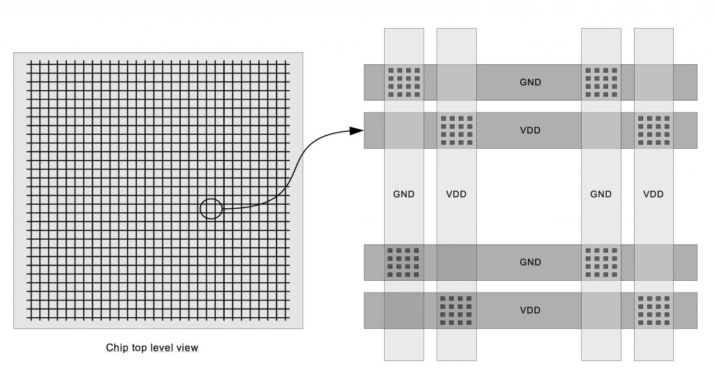
Figure 1. A typical Power Grid
Basically, the power grid should be uniform on the whole chip but some discontinuities may be introduced to better control the power consumption of the chip. Power gating is now commonly used in System On Chip design.[7] This technique allows to completely disconnect some parts of the system in order to reduce leakage consumption. This implies, in some specific case to build separate power grids. We then have “isolated” grids that are not directly connected by metal stripes, but through power switching transistors.
The following schematic shows different ways of distributing power among different blocks. Switching can be made either between the top level power grid and the block level power grid or directly at top level. In this second case, it is expected to have power line interruptions. This particular case will need to be taken into account during final validation.
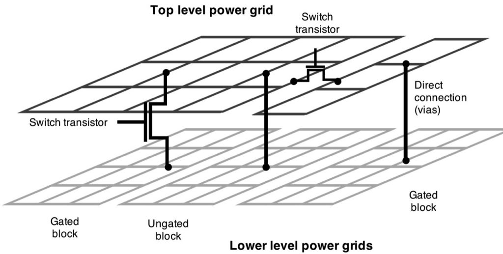 Figure 2. Gated power grids
THE CHOSEN SOLUTION
Pure geometrical validation
Finally, it appeared that the top level power distribution could be validated by pure geometric rules. The time consumption and the computing power required by a netlist extractor could be spared. As this analysis has to be made flat, because the power grid itself was drawn flat at top level, there was no advantage to use a hierarchical tool. It has become obvious, due to similarities of the analysis, to orient our efforts to the use of a tool dedicated to physical level processing. We thus decided to use a mask rule checker which offered the best performances and all the expected features and capabilities to perform the requested checks. The definition and the setup of the analysis rules was also much more convenient to adjust.
Vias counting
The first issue we had to detect was the number of vias present at the intersection of a vertical and an horizontal power line. In order to reduce the resistivity of connections between the two metal layers dedicated to power distribution, a maximum number of vias should be arrayed at each layer intersection. As the width of power stripes is constant because of the uniform power consumption, it is easy to deduce the expected number of vias at each intersection.
Next figure shows some example of electrical problems which could not be detected by a Layout vs Schematic tool. Indeed, all the electrical connections exists and are functional, but parasitic resistors could lead to some critical power breakdown.
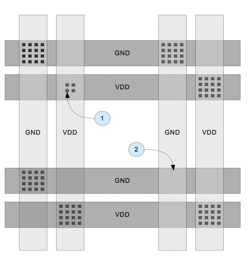
Figure 3. Missing vias
| Configuration | Type of error |
|---|---|
| Case 1 | High resistivity connection due to reduced number of vias |
| Case 2 | No direct electrical connection due to missing vias |
It must be noticed that some intersections have no vias. Only the intersection of an horizontal VDD with a vertical one, or the intersection of a vertical GND with an horizontal one should be covered with arrays of vias. Without the use of a netlist, it becomes more difficult to identify the expected missing vias from unexpected ones. Different solutions has been found to fix this issue.
The first one consisted in identifying GND and VDD dedicated wires on the layout. This can be easily made by using a specific datatype for the related metal level. For example, if layer 100 datatype 0 is the level number of upper metal layer, we can use layer 100 datatype 1 for GND and layer 100 datatype 2 for VDD. Number 100 datatype 0 remaining for any other type of signal. This technique greatly simplify all above mentioned checking as well as short detection. Finding a short with a Layout vs. Schematic tool is often a nightmare for the designer. If power usage of the wires are properly identified, detection of a short can be easily an quickly detected by a pure geometric analysis tool (i.e. Design Rule Checker). Any intersection of a metal dedicated to VDD with a via and a metal dedicated to GND is a short.
The second solution was not based on the mechanism of layer usage recognition but was less reliable. It was based on the fact that there is normally the same number of intersection on both power grids (i.e. VDD and GND). If the number of intersections in which no vias were found was different of the number of intersections in which some vias were found, there should be a Design error.
However, in both cases, each intersection with a number of vias different from 0 and from the maximum value is an error. A simple option of the mask rule checker used for this analysis allowed us to get a report with the summary of vias counting.
Here is the simple code to count vias:
INPUT1 : Metal-1
INPUT2 : Metal-2
INPUT3 : VIA
AND INPUT1 INPUT2 lay_intersect ;
INTERACT INPUT3 lay_intersect lay_via ;
SUB lay_via lay_intersect OUTPUT1 ;
INTERACT lay_intersect lay_via OUTPUT1 int_rule ;
int_rule { INTERACT_RULE = (0, n=0) (1, n=1) (2, n=2) (3, n=3) (4, n=4) …(x, n>=x) ; }
Where x is the maximum number of vias in the intersection.
Next table shows the type of report obtained after running the Mask Rule Checker.
| Vias count | #occurrence | comment |
|---|---|---|
| 16 | 6 | As expected |
| 4 | 1 | Should be an error |
| 0 | 7 | Should be an error |
Line interruptions
At this level, because we had no any netlist information, it was not possible to determine whether two power lines to be connected or not. Next figure shows different kind of power lines interruptions.
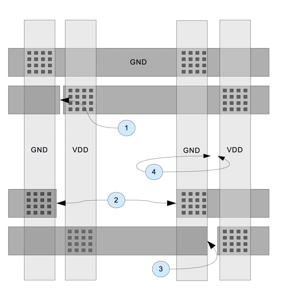
Figure 4. Power line interruptions
| Configuration | Error |
|---|---|
| Case 1 | Line interruption detected by a classical DRC (if spacing < minimum) |
| Case 2 | Considered as an expected power line interruption |
| Case 3 | Unexpected line interruption (not detected by a DRC) |
| Case 4 | Not a line interruption (same spacing than case 3, but parallel lines) |
A line interruption is defined by a gap between two facing edges of two wires on the same layer (case 1 and 3). The facing edges should be on the width (smaller side) of the metal wire. The gap should be smaller enoughnot to be considered as an expected interruption (case 2). A gap between the “long” side of two wires is not considered as a line interruption (case 4). The two lines are two separate power connections.
If the gap is very small (case 1), i.e. smaller that the min spacing defined in the design rule manual, the interruption will be detected by the DRC. Thanks to the advanced options of the MRC it was also possible to detect line interruptions as shown in case 3.
Here is an example of the simple code to detect interruptions of less than 1000nm on Metal-1 lines:
INPUT1 : Metal-1
MRC INPUT1 OUTPUT rule;
rule { SPACE_RULE = (1, h=*, s< 1000, DIFFPOL); }
Results
Performances
A mask rule checker, such as the tool that has been used, works with a flat representation of the design. This may be considered as a problem as the database is hierarchical, and thus, may lead to dramatically increase its size. But after a detailed study of the chip representation, it appeared that the power grid was designed almost flat and was made of a large cell covering all the die. In this case, there is almost no difference in terms of computations, between a hierarchical or a flat analysis. Additionally the Mask Rule Checker splits the full layout into windows to avoid to use too much memory and its algorithms have been specifically developed to reach the best performances on flat databases.
The full scan of the GDSII database, which was 35Gb large, took around 30 minutes for each validation, i.e. vias counting and line interrupt detection.
Manual analysis
Once completed, the Mask Rule Checker has identified about 20 line interruption. The detailed analysis must have been performed manually to check if these gaps have been intentionally inserted or not in the power analysis. For power consumption reduction, some parts of the design can be disconnected from power supply. Power distribution is made through a dedicated power switch and the power grid of the related block is then disconnected from the standard power grid. The detailed manual analysis allowed to validate that each detected line interruption was expected and made for above mentioned reasons.
Acknowledgments
We would like to warmly thanks Kalray’s (KALRAY) design team for their collaboration in the validation of our layout finishing flow as well as the developers of SmartMRC who helped us for the setup of the configuration files for the Mask Rule Checker. Getting a first time good silicon on such a complex chip is the best recognition we all can have expected.
Conclusion
Any CAD tool has some limitations in terms of performance and efficiency. Setting up the design flow of a very complex chip on the most advanced technology requires to use each tool at its best. This means that the choice of the methodology must take into account, not only the expected result but also the performances of each tool. With this case study, we then have used a Mask Rule Checker to perform electrical checks. This non standard usage has led to a great improvement on the validation time of the final chip. Innovation may also come from a shifted approach of the analysis of a new challenge. The reuse of well known tools and methodologies into a different context can be fruitful.
REFERENCES
[1] N.H. Abdul Ghani and F.N. Najm. Fast vectorless power grid verification using an approximate inverse technique. In Design Automation Conference, 2009. DAC ’09. 46th ACM/IEEE, pages 184–189, 2009.
[2]. Abhishek. Incremental power grid verification. In Proceedings of the 49th Design Automation Conference, DAC ’12, New York, NY, USA, 2012. ACM.
[3]. Space Daily. European investments in advanced computing systems deliver results, february 2013.
[4]. John Goodenough and Rob Aitken. Post-silicon is too late avoiding the $50 million paperweight starts with validated designs. In Proceedings of the 47th Design Automation Conference, DAC ’10, pages 8–11, New
York, NY, USA, 2010. ACM.
[5]. Chi-Wen Pan and Yu-Min Lee. Redundant via insertion under timing constraints. In Quality Electronic
Design (ISQED), 2011 12th International Symposium on, pages 1–7, 2011.
[6]. Mondira (Mandy) Deb Pant. Microprocessor power delivery challenges in the nano-era. In Proceedings of the
16th ACM/IEEE international symposium on Low power electronics and design, ISLPED ’10, pages 375–376,
New York, NY, USA, 2010. ACM.
[7]. Youngsoo Shin, Jun Seomun, Kyu-Myung Choi, and Takayasu Sakurai. Power gating: Circuits, design
methodologies, and best practice for standard-cell vlsi designs. ACM Trans. Des. Autom. Electron. Syst., 15(4):28:1–28:37, October 2010.
-
Categories
- Glossary
- Publications
- Resources
- Whitepapers